If you want to send video and audio signals are spread to multiple televisions simultaneously.
You may use a Video amplifier splitter by transistor BD137-BC547-BC557 circuits.
But it is limited. The need for wiring and is only about 4 set only.
Let’s try this circuit is DIY The wireless video & audio signal sender. Can be used with a television receiver is not limited. And wireless systems. Distance is about 40 feet. And important this circuit small device. So is not difficult to create.
The working principle
??Block diagram of wireless audio video sender consists of as follows.
1. A main frequency generator acts to produced the signal carrier of the television signal. And is the main frequency of this project.
2. A signal amplifier will amplify signal come from the frequency generator circuit to up enough to can drive a power amplifier circuit.
3. A frequency generator in VCO form, will produce a center frequency 5.5 MHz. Which this frequency will change by a input signal, contributes to the FM modulated by a television signal system.
4. This power amplifiers in addition to the high-power amplifier is the last time before it was broadcast. Also acts as a modulated video signal and audio. (Through the FM modulation) mixes with Signal carrier frequency of the video signal in the AM as well.

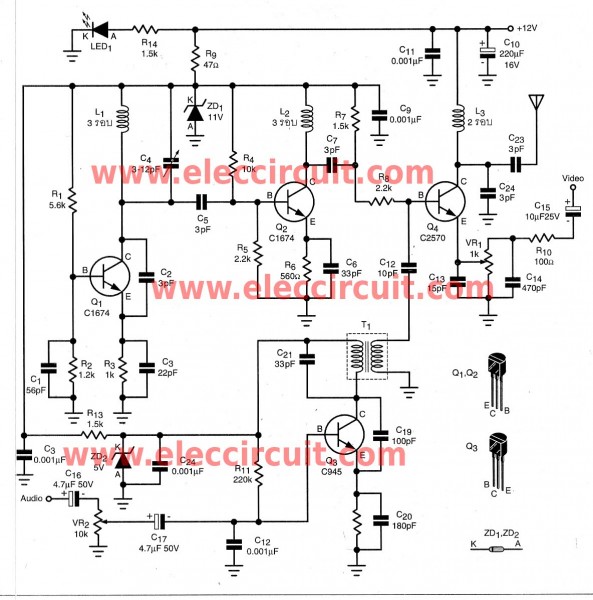
The wireless audio video sender circuit is shown in figure 1. The main frequency generator circuit in form of LC in a ground-base configure type. By has L1 and trimmer C4(3-12pF) together to into a tuning circuit at output.
For adjust the video signal carrier frequency as you need in range of 450MHz-550MHz. The R1, R2, R3 are a bias circuits to Q1(C1674). By has C1 cut a high frequency at pin base. Both capacitors C2 and C3 are connected as divider circuit to determine rate of signal that feed back from collector to emitter. The C3 so is not the bypass signal capacitor as general case.
This frequency is send to amplify up by through coupling capacitor C5 to transistor Q2(C1674) that is the signal amplifier circuit, The resistors R4,R5,R6 are set to the bias circuit to Q2, a capacitor C6 is capacitor bypass frequency to the ground, to protect the loss of power at the R6.
The inductor L2 send the DC voltage to Q2 At the same time, it was a RF Shock, prevent visual Signal carrier frequency, output to supply it.
Since we want to have a frequency stability over power. We make regulation the power supply circuit to this the second input sector. With zener diode ZD1 by has value R9 is limit current and filter to smooth with two capacitors C8 and C9, The signal is amplified through the link on the capacitor C7 ,to Q4 that is power amplifier circuit and AM modulation circuit with the same time, by will be reduce by the resistor R8 to the appropriate size for the audio signal to pass through the base pin of Q4. The same R7 and R8 are the bias resistors to Q4 . The inductor L3 act same as L2 and because this sector we want the best power than others , The power supply for this ,so come direct from the main power supply. By have capacitors C10,C11 and C23 are filter current for the signal that is modulated with the video carrier wave, ready with the sound signal in AM form that will be coupling and adjust the amplitude of signal suitably with C13,C14,C15 and R10, by has the VR1 is used to adjust percentage of modulation. The audio signal will be coupling through C14 and C17 go to the Q3, by has VR2 adjust the range frequency deviation
Both R11,R12 are the bias resistors. The C18 is cut off high frequency on pin base. C19 and C20 are the divider capacitors as same C2,C3, that is set as the generator circuit on LC ground, base and configure same with Q1. But the circuit is determined as VCO(voltage control oscillator) to modulated the audio signal that into the FM input, by Center frequency of 5.5MHz, which is the frequency difference between the Signal carrier frequency video signal with audio carrier signal. The set of values of T1 and C21.
The audio signals through the FM modulation through T1 and C12 are the coupling pin to the base of Q4. The power supply that entered to this section will be regulaed as 5 volts by zener diode ZD2, has R3 is limiter current and filter to smoothed do not the high frequency within by C22. The television signal is completed form outout of Q4 will be sened Will be spread broadcast antenna, the capacitors C24 and C25 act as the matching circuits. For the status of the device is indicated by LED1, with limit current by R14.
 The PCB Layout for builds
Related Posts :
-
This is the video amplifier circuit or the video splitter circuit, it is designed to take video signal is stronger. Compensate for the loss of signal, and is video splitter video, which can connec ...
-
This the fm wireless transmitter circuit, the truth is one kind microphone that developed to be used without a cable from the microphone to the amplifier. Makes flexible to use than a plain microp ...
-
“Compact portable AM radio with plain headphones.” You've probably seen a small radio with earphones. You can put it in your pocket. This project is similar, but the small little device. Its eas ...
-
This circuit is FM radio receiver that very small size and works well, although the sensitivity is poor. The principle of this circuit is to use the generator frequency circuit. Which consists of ...
-
A tri-amplifier has three in one a amplification act drive specifically each audio speakers makes the sound quality is very good. Normally amp can drive three speakers at the same time are th ...


